
PCB SMD Typesetting Turkey
PCB SMD Typesetting: Everything You Need to Know
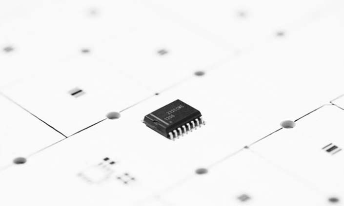
Surface mount technology (SMT) has revolutionized the electronics industry, allowing for smaller and more complex printed circuit board (PCB) designs. One of the key aspects of SMT is PCB SMD typesetting, which involves the placement and orientation of surface mount devices (SMDs) on a PCB.
In this blog post, we will cover everything you need to know about PCB SMD typesetting, including its benefits, challenges, and best practices.
Benefits of PCB SMD Typesetting
Before we dive into the details, let’s first discuss the benefits of PCB SMD typesetting:
1. Space Saving
SMT components are much smaller than their through-hole counterparts, allowing for more compact PCB designs. This is especially important for portable and wearable devices where space is at a premium.
2. Improved Performance
SMT components offer better electrical performance due to shorter signal paths and reduced parasitic capacitance and inductance.
3. Higher Reliability
SMT components are less prone to mechanical stress and thermal shock, resulting in higher reliability and longer lifespan.
4. Lower Cost
SMT components are cheaper to manufacture and assemble, resulting in lower overall production costs.
Challenges of PCB SMD Typesetting
Despite the numerous benefits, PCB SMD typesetting also poses several challenges:
1. Component Size
SMT components are much smaller than through-hole components, making them more difficult to handle and place accurately.
2. Component Orientation
Unlike through-hole components, which have a fixed orientation, SMT components can be placed in multiple orientations, making it crucial to ensure correct placement.
3. Soldering
SMT components require precise soldering techniques, including the use of solder paste and reflow ovens, which can be difficult and time-consuming.
4. Inspection
Due to their small size and complex orientation, SMT components can be difficult to inspect for defects, making quality control and testing crucial.
Best Practices for PCB SMD Typesetting
To overcome the challenges of PCB SMD typesetting and ensure high quality, reliable PCBs, the following best practices should be followed:
1. Use Design Software
Use PCB design software, such as Altium, Eagle, or KiCAD, to design SMT footprints and ensure accurate placement and orientation.
2. Follow Manufacturer Guidelines
Follow the manufacturer’s guidelines for component placement and orientation, and use their recommended soldering techniques and equipment.
3. Check for DFM Issues
Check for design for manufacturability (DFM) issues, such as incorrect pad sizes, spacing, and clearances, to ensure smooth assembly and production.
4. Use Automated Inspection
Use automated inspection techniques, such as X-ray and optical inspection, to detect defects and ensure high quality.
5. Test and Debug
Test and debug the PCB thoroughly before mass production to ensure proper functionality and performance.
Conclusion
PCB SMD typesetting is a critical aspect of SMT assembly, enabling smaller, more complex, and higher performing PCB designs. While it poses several challenges, following best practices and guidelines can ensure high quality, reliable PCBs.
—
For Germany, there is a company based in Turkey that offers PCB assembly services, including SMD typesetting. One such company is Teknik Elektronik A.S. , which has been providing SMD assembly services for more than 20 years and has modern and powerful machines for precise and cost-effective assembly of PCBs with surface-mounted devices.Sh. it is his company.
—
Cities in Germany where we provide smd typesetting and PCB assembly services.
Berlin, Hamburg, Cologne Munich and other cities.
To get pcb production and pcb typesetting and assembly services from Turkey, please contact us by e-mail. our e-mail address is info @ teknikelectronics. com
—